|
|
||
|
LM5025A Die |
||
| Active Clamp Voltage Mode PWM Controller | ||
| Fabrication Attributes | General Die Information |  |
||
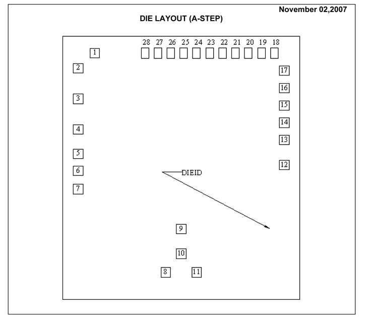
| Physical Die Identification |
LM5025A | Bond Pad Opening Size (min) | 91μm x 91μm | |
| Die Step | A | Bond Pad Metalization | Al_ 0.5%Cu | |
| Physical Attributes | Passivation | PECVDOX+NITRIDE | ||
| Wafer Diameter | 150mm | Back Side Metal | BARE BACK | |
| Die Size (Drawn) | 2286μm x 2540μm 90.0mils x 100.0mils | Back Side Connection | Floating | |
| Thickness | 254μm Nominal | |||
| Min Pitch | 167μm Nominal | |||
| Special Assembly Requirements: | ||||
| Note: Actual die size is rounded to the nearest micron. | ||||
| LM5025 MDC MWC ACTIVE CLAMP VOLTAGE MODE PWM CONTROLLER  |
||||